The history of the Industrial Institute of Electronics (PIE) are inseparably connected with Zaklady Wytworcze Lamp Elektrycznych them. Rosa Luxemburg (ZWLE) - a factory of electron tubes.
On the initiative of the director of ZWLE-docent (later professor) Wieslaw Barwicz (1913-2002), on 1 July 1956, the Central Electronics Laboratory
was transformed into the Industrial Institute of Electronics (Przemysłowy Instytut Elektroniki- PIE). The first long-time director of PIE was the aforementioned prof. Wieslaw Barwicz,
who was the author of several books dealing with electron tube technology as well as electron beam applications.
In 1957, the publication entitled "Fundamentals of construction and technology of electron tubes" was published by PWT.
In 1974, the book "Application of electron beams in industry and in scientific research" (Unitra),
in 1989 was publishe the book "The electron beam in industry" appeared.
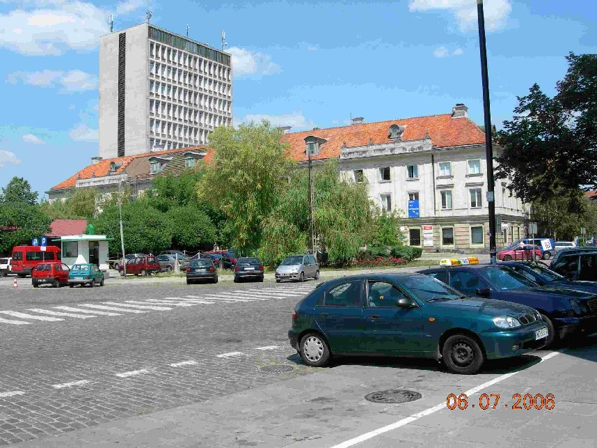
Industrial Institute od Electronics (headquarters) was located from the beginning to the end of its existence at ul. Dluga 44/50 in Warsaw (next to the "Ratusz" tube station).
The past of this building is not entirely clear and is shrouded in legend. The building was built after the second war. In the neighborhood - on the side of the building,
practically in the Krasiński park there are ruins of the so-called Simons' passage. In 1956, the building was put at the disposal of PIE.
Previously, there was a prison or detention here, as evidenced by the cellar's preserved cells here and there. There are also visible judaas or holes after them;
in the cells above the door there is a barred hole for the bulb. Some of the rooms are tiled. Remains of showers in the corridor have also been preserved.
Unconfirmed rumors say that at this point there was one of many prisons in the Security Police (MBP, UB), which became unnecessary during the period of de-Stalinization.
Tiles made it easier to keep clean after interrogation - it was easier to wash blood from them. According to some, the building was supposed to have a secret passage
- a tunnel connecting with the Mostowski Palace. This legend was supposedly created after a "outhouse" toilet fell in the corner of the property from the side
of the Krasinscy park. The PIE testing plant, which no longer exists, was located nearby at ul. Bielańska 10. From the beginning of its existence,
the subject was connected with semiconductors at the Industrial Electronics Institute.I had this information from Professor Andrzej Czachor (1934- 2017), who participated in the initial period of work on semiconductors at PIE.
With Professor Andrzej Czachor from the National Center for Nuclear Research (NCBJ), I used to travel on average twice a week. For the first time,
when on Thursday morning the institute coach takes employees to the institute and the second time, when the same coach drives workers back home in the afternoon.
Some years ago in the summer, when we were returning home as a member of the Institute for Nuclear Studies (IPJ), to extract the time, I took my old newspapers from
the Industrial Institute of Electronics (PIE) from the 1950s and 1960s. on the seat next to sat prof. Andrzej Czachor and casually looked at my reading.
He then confessed to me that he started his professional career at PIE in 1956 and was involved in measuring the properties of semiconductors.
At that time, I took this information quite coldly, as not very interesting to me. The situation changed when I learned about the death of prof. Witold Rosiński
- the senior of Polish semiconductor electronics. At that time I understood that this is the last moment to gather information about the beginnings of semiconductors
in Poland. I promised myself that I would write down what prof. Andrzej Czachor has a say in this topic. Recently, in April 2013, such an opportunity came
and I visited Professor in his office. My interlocutor claimed that he did not have a very good memory and that it was easier to recall certain episodes.
- I started working at PIE in 1956. I went to the plant of Mrs. Morkowska. I also remember from this plant Mr. Nast. At the same time, other physics
graduates went to the plant with me: the late prof. Jerzy Piekoszewski (from Poznan), Marian Kozielski (from Torun) and Eugeniusz Szyszko (from Poznan).
Marian Kozielski was involved in breeding monocrystals. We all came to PIE with the so-called work order.
The group we came across dealt with semiconductor materials (imported from abroad). I do not remember exactly, but it seems to me that it was Germanium.
The test materials were cut with wires immersed in a suspension of carborundum powder. Diode rectifiers were made of such cut plates.
I remember that the transistor case was then in the viewfinder. Around this time, Shockley's book appeared and it was a basic reading for us.
It was difficult for us - graduates of physics. It was necessary to change the thinking of electrons in vacuums for holes and electrons in a solid body,
and it was not so easy. Mrs Kazimiera Morkowska was entitled "Doctor" and she was older than us.
At the beginning of 1958, our team continued work on creating a stand for drawing single crystals using the Czochralski method.
I have personally seen the first single crystal from this device, similar to the propeller rather than the rod.
At that time, we were convinced that it was the first monocrystal in the country, pulled out with this method and the atmosphere was elevated.
As for my role in the team, I was a theoretician. I dealt with measurements (including a four-probe for measuring the semiconductor resistance
and apparatus for measuring the lifetime of carriers, constructed by engineer Chmielewski). However, I reserve the fact that I did not recognize
the designer personally. He left the band probably in front of my academy. As for the construction of this last device, it worked as follows:
A light spot from an incandescent platinum wire was projected onto a smoothed semiconductor surface. In the vicinity of the spot there was an electric
contact which transferred the generated voltage to the amplifier. This tension was the smaller, the greater the distance from this spot and the shorter
the life span. The curves representing the dependence of voltage on the distance of the spot from the contact were the Bessel functions.
Having standardized curves for several lifetimes (10, 50, 100 microseconds) it was possible to make a comparison and on this basis the time of life of the carriers
in the sample was determined. Initially, the light spot was a line. After some time I improved the device, so that the spot was a point and then the measurement
was radial, and the solution was an elementary function. In the first half of 1958, I felt that I was not developing anymore. Under the influence
of prof. Piekoszewski, who moved to IBJ earlier, I also decided to move there. As for the location of our studio in PIE, it was located on the first
floor of the building at ul. Długa 44/50 and occupied the first two windows from the side of the Krasińscy park, looking from ul. Ghetto Heroes.
I remember that for reasons of renovation, we were probably moved at the beginning of 1958 to ul. Stepinska
(There used to be the Experimental Institute of Semiconductors - my note). I remember that there was a woman there - a technician who had short tubes
a few millimeters in diameter and massively inserted a set of wires with contacts on the semiconductor wafer and immersed the tubes on the small
but sharp flame of the burner. She did a lot of it! Every day, at least 200-300 pieces of such sets closed. I remember, however, that this lady did
not have a sense of mission (my interlocutor probably mentions the process of producing the first series of DOG diodes - my note).
The equipment for our research was made by the institute's employees. I do not remember that we would do some shopping from abroad.
Eugeniusz Szyszko, who later moved to TEWA, made a great contribution to creating the apparatus. I do not currently have
contact with him and I do not know if he is still alive. As you can see from the professor's account, the topic of semiconductors
was taken up early, but also from the institute in the beginning, it basically "traveled" to TEWA. Therefore, the first 15 years of operation
of the Industrial Electronics Institute is mainly associated with electronic tubes.
The reconstruction of PIE's oldest period of existence (1956-1971) is not an easy task. The reason for this state of affairs is the fact that the chronicles kept in PIE went to either the milling or the archives of new files. Burial in these documents will be a task for the historian. From the transcripts, it is impossible to decipher what materials were actually transferred to the archives. The existence of these chronicles, supposedly richly illustrated with photographs, has been confirmed by two people. I have (unfortunately only!) An analysis of copies of "Electronics" available in my library - initially the Technical Bulletin of Zakłady Wytwórczych Lamp Elektycznych im. Rosa Luxemburg, a publishing house that was later transformed into "Works of the Industrial Institute of Electronics", issued until the end of the Institute's existence. I can also rely on other materials that have passed me by the hand of luck. At the beginning, however, I will discuss the contents of "Electronics" notebooks in general, to be able to summarize, probably incomplete.
The reconstruction of PIE's oldest period of existence (1956-1971) is not an easy task. The reason for this state of affairs is
the fact that the chronicles kept in PIE went to either the milling or the archives of new files.
Burial in these documents will be a task for the historian. From the transcripts, it is impossible to decipher what materials were actually
transferred to the archives. The existence of these chronicles, supposedly richly illustrated with photographs, has been confirmed by two people.
I have (unfortunately only!) An analysis of copies of "Electronics" available in my library - initially the Technical Bulletin of
Zakłady Wytworcze Lamp Elektycznych im. Rosa Luxemburg, a publishing house that was later transformed into "Works of the Industrial Institute of Electronics",
issued until the end of the Institute's existence. I can also rely on other materials that have passed me by the hand of luck. At the beginning, however,
I will discuss the contents of "Electronics" notebooks in general, to be able to summarize, probably incomplete.
I have also number 6 from this year. The number 1-2 from 1958 is already named "Elektronika Biuletyn Techniczny Przemyslowego Instytutu Elektroniki".
There is an article by Aleksander Braginski entitled "magnetic materials" and an article by Jerzy Pultorak from ZE IPPT PAN (should it be Electronics?).
"Blade-lay transistor". Number 3 contains an article by Alfred Krolikowski from PIE about storage tubes.
The number 8 contains an article by Szymon Firkowicz (a specialist in the field of reliability evaluation of electronic components)
from PIE entitled "Some issues of modern technology of low power electron tubes in the light of their competition with transistors"
and an article by Antoni Kilinski from the Department of Telecommunications Constructions and Radio Broadcasting at the Warsaw University of Technology.
It seems that in 1959 the notebooks of the "Electronics" series did not appear at all. The number 1 from 1960 is already called
"Prace Przemyslowego Instytutu Elektroniki". The editorial board at that time was significantly limited.
However, from that year on, a good custom of writing, in addition to the authors' names, was also given to the name of the PIE studio in which they were working.
Due to to this, we can say something about the PIE structure, although, for example, it is difficult to say something more about experimental plants,
whose employees have little or no publication. From the reading of notebooks we know that in 1960 in PIE there was an Independent Workshop of vidicons and photomultipiers
, Independent Workshop of microwave tubes and the Department of Physics of Electron tubes.
From the number 1/1961 we learn about the existence of the Independent Subminiature Laboratory in Wroclaw (miniature electrometric tubes were created there),
Workshop of pkotocathodesin Torun (within the Electron Tubes Department), Laboratory of Theoretical Issues (within the Department of Physic of Electron Tubes),
Department of Vacuum Metals.
From issue 2/1961, we learn about the existence of the Workshop of Materials for Tubes in Wroclaw, the Department of Radiotechnics and the Experimental Station PIE
- Department of Construction of Measuring Instruments.
On the other hand, from No. 2/1962, we learn about the existence of an Independent Workshop of Pure Metals,
and from No. 3 about the existence of the Image converting tubes, the Chemical Technology Department, the Ceramic Tubes and Long-live tubes.
From the first issue from 1964, we learn about the existence of the Emission Testing Department, the Vacuum Physics Plant,
and the Department of gas filled tubes. From the number 4/1964, we learn about the existence of the Independent Glass Laboratory and the
Independent Analysis Laboratory.
In the number 1/1965, we learn about the existence of the Medium-Power Microwave Tube Plant and the Electron-Metrology Department
and the Department of Solid State Physics. In the issue 3-4 / 1966, we refer to the Independent Getter's Laboratory and the Ceramic Joints and Applications Center.
From the number 2-3 / 1969 we infer about the existence of the Materials Research Department.
On the other hand, in the 2/1970 issue, the Vacuum Technology Plant appears. The authors formerly were in the structure of the Department
of Electronic Lamp Physics.
The number 3/1970 refers to the Department of Lamp Technology of Photographs; in the 3-4 number from 1971,
the Experimental Department of Technological Equipment and the Experimental Department of the Industrial Electronics Institute in Torun appear.
This is where the publishing house "PIE works" ends until 1972, ie until the moment of serious reorganization, as will be discussed later. Summary:
The first years of PIE's existence (1956-1958) were the period when both the work on electron tubes and semiconductors were carried out at the Institute.
The production of semiconductor materials, but also semiconductor components originated in addition to IPPT PAN also from ZWLE im. R. Luxembourg.
This apparent paradox can be explained by the fact that vacuum devices are necessary during the production of semiconductors.
It is obvious that the richest vacuum equipment at that time had just ZWLE. The first year includes a lot of translations of foreign literature and
the work of Polish scientists outside PIE. It seems that in this way, at least part of the publishing gap has been tried to fill the market.
The annual break in publishing the PIE Bulletin (1959) and the subsequent limitation of the editorial board are a puzzling one.
Perhaps this was due to the separation of the group of "semiconductors" to the then PEWA with the presumed seat at Stepinska street. Interestingly,
not all semiconductor topics have been given away. The constructions of Hallotrons or photooporators of the FOK series were created in PIE around 1960
and for a few years they were produced by the Torun branch of the PIE. It seems, therefore, that only a group dealing with diodes,
transistors and some aspects of metrology has been separated into PEWA. In the Torun branch, the phenomenon of electroluminescence of sulphides under
the influence of a changing electric field was also tried. Anyway, it seems that at Dluga street 44/50 there were no traces of the former "semiconductor activity"
of the 1950s. At least I have never encountered such a thing. By the way, the rooms occupied by "semiconductors"
have been repeatedly adapted for new purposes. It is known that around 1959 the Institute undertook the production of ELW1 tubes, equivalent to E1T western tubes
(manufactured, among others, by Philips). These tubes were manufactured in the PIE Experimental Station at Elekcyjna street number 106
(later there was a change of address on Ciolka street, but this is probably the same location).
At the beginning of the 1960s, a Polish vidicon type PWM2 for the purposes of black and white television television was developed at PIE.
In the following years new versions of the widic were created, marked with symbols PWM21, PWM3, PWM4, PWM6.
More information about these analyzing tubes can be found on my website. An interesting article by Aleksander Fryszman and Ewa Zarzycka in "PIE's Works"
about the way in which structural problems were solved in the development of phantoms came from 1960.
From the reading of the PIE notebooks, it appears that throughout the 1960s the most powerful was the Department of physics of electron tubes. The most employees
wrote this plant. The Vacuum Technique Department and perhaps other departments have probably separated out of it.
During this period, the leading subject was the understanding of the composition of the vacuum atmosphere, the amount and type of gases released,
new types of cathodes and the associated development of mass spectrometry (mainly using omegatron).
The research carried out with its use allowed to explain to a large extent the reasons limiting the durability of electron tubes,
caused by the influence of residual gases on oxide cathodes, commonly used in electron tubes.
Later, as part of OBREP's (created from PIE in 1972) activity, helium leak detector HWN1, quadrupole mass spectrometers of the QSM series as well as ionic guns
were developed. At the same time, with the development of lamps, it became necessary to develop a vacuum technique. At the Institute, ionizing
probes for measuring the vacuum, ion-sorption pumps were developed. This work was led by the team of Wenancjusz Czarycki.
It seems that attempts have been made to construct an image orthicon - an analyzing tube for television. As far as the construction of the widget
went around 1960 and it was produced in different versions in PIE, then in OBREP, DOLAM and Zaklad Lamp Profesjonalnych (in Polkolor structures)
until the end of the 80s (so for about 30 years), ortikonu probably did not manage to do. However, attempts were made to make details
(an article about the image grid).
One work from the mid-1960s relates to ionizing radiation detectors that are known to have been produced in the PIE Experimental Station at Elekcyjna (later Ciołka) street
in Warsaw from at least 1959, probably until the end of the 1980s (later as part of OBREP). Around 1963, the team headed by prof. Barwicz implemented Polish version "Nixie" tubes
marked LC1. From this tube come later, more well-known types, eg LC513, LC531, produced in the "DOLAM" factory in Wroclaw.
An interesting fact is that the professor has developed an elaborate lamp - analog-digital converter for digital voltmeters.
The incoming semiconductor technology soon replaced the tubes. Among the other lamps developed at the Institute, one should mention thyratrons,
gasotrons, trigger tubes, trigger electrometric tubes for use in fire detectors (!) with the PZ2E designation. These successful solutions were
developed by a team of docs. Henryk Poniewierski. We owe him also the national reed switches and the subsequent extinguishing chambers.
The colorful CRT tube is a mystery. In PIE's notebooks there is a superior foreign official. One, a retired employee who started his career in ZWLE,
claimed that before the PIE was created, attempts were made in ZWLE in this direction.
The 1960s were the development of ceramic lamps and reliability theories. The end of the 1960s brings less work in the field of lamps, but more from vacuum techniques,
ion pumps, pluggers or electron beam technology. This subject remained until the end of 1971 and was then continued in OBREP.
On January 1, 1972, the division into OBREP and PIE (included in the NPCP CEMI structure). This event marks the first period of the existence
of the Industrial Institute of Electronics.
It is worth mentioning here that in 1971 the ONPMP - Scientific and Production Center of Semiconductor Materials was created, transformed in 1979
into the Institute of Electronic Materials Technology. It is known from oral history that some of the employees of the former PIE have just passed to the ONPMP.
The migration of employees between institutes was, moreover, multidirectional. Later, some went, for example, from ONPMP to OBREP.
The fate of this part of the PIE connected with the vacuum was really changeable and quite intricate. In the years 1972-1977, it was separated from PIE OBREP
(Research and Development Center for Vacuum Electronics). In 1977, OBREP was transformed into OBRTT (Research and Development Center for Television Techniques).
However, this name also did not last long. In the years 1980-1984, the name of OBRPO (Research and Development Center for Image Transducers) was in force.
In 1984, the old name OBREP was returned, which survived until 1993. This year ITP (Institute of Vacuum Technology) was established, which operated until 2002.
In 2002, ITP was incorporated into the PIE.
In addition, branches in Wroclaw, Koszalin and Torun were separated from PIE, which was still in the 1960s. Experimental plants were also set up
(among others Experimental Factory of Electron Tubes "DOLAM" in Wrocław, ZAP in Boleslawiec). As it has already been mentioned, the Industrial Institute of
Electronics gave birth to the Semiconductor Materials Center (today it is the Institute of Electronic Materials Technology ITME in Warsaw)
and also the TEWA semiconductor factory (later transformed into CEMI (now no longer existing Scientific-Production Center of Semiconductors).
In 1970, the mentioned CEMI was created. In 1971, PIE became part of this Center as a subordinate unit. In the years 1971-1991,
PIE was the research and development base of our semiconductor industry. The institute has developed diffusion stations, automation devices
for assembling integrated circuits and integrated circuit testers. Liquidation of CEMI limited the development of PIE's activity in this direction.
The political changes forced the need to change PIE's activity and the need to reconnect PIE with ITP (former OBREP).
On September 1, 2007, PIE was consolidated with the Tele- and Radiotechnology Institute (ITR), taking the ITR name.
The Institute's current activity (initiated in PIE) includes, among others, quality testing and calibration of electronic products
(accredited laboratory), development and production of electric heating devices and laboratory furnaces, temperature regulators and thermo-chemical controllers,
and measuring systems for medical diagnostics, electron beam welding machines.
The vacuum technique center runs, among others the following activities:
Back to main page